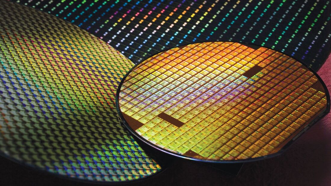
 GaN Epitaxial Wafers GaN Epitaxial Wafers are a kind of semiconductor epitaxial wafers that are designed with the help of epitaxial growth procedure. These wafers are utilized in power electronics, LEDs, and other appliances. These GaN Epitaxial Wafers are contrived by the growth of epitaxial on substrates that consist semiconductor single crystal substance.
GaN Epitaxial Wafers are further designed into semiconductor chips and other appliances. Higher electron movement, low transferring loss, and fewer lattice disparities are some of the benefits of gallium nitride that make it a unique substance for higher-efficacy power electronics. This is particularly factual in high-voltage Direct Current/Alternate Current and Alternate Current / Direct Current power electronics, where the capability to work at higher frequency is a vital benefit of GaN compared to silica and silicon carbide elements. Anyhow, GaN has not been well advanced in free-standing wafer technique, owing to its high lattice mismatch and thermal extension coefficient variance from silica and SiC. It needs a heteroepitaxial development technique that manages stress and density deficiency, and which is appropriate for the huge productivity and price needed for GaN-based elements. A group from the Naval Research Laboratory US and its commercial collaborators have advanced a new method to develop thick GaN film on permeable silicon additives utilizing high-vacuum epitaxial growth. This new substrate model enables scientists to develop a budget-friendly wafer with minimal working of the element. This research outcomes in a Gan Epitaxial Wafers with a lower defect density and huge quality crystalline development, which can be utilized to make huge-efficacy Light Emitting Diodes and other higher-voltage semiconductors. It also offers an essential platform for GaN-related survey into conductive oxides that can be employed to enhance device performance, rises efficacy and reduces the usage of power. The GaN epitaxial wafer must be a higher-quality wafer as it wants to be capable to manage the high frequency, so it must have a high dislocation density and be stably thermal. Generally, GaN epitaxial wafer equipment have been developed on costly SiC substrates. Orderly to create and produce optoelectronic and electronic equipment on GaN wafers, crystal standard must be more. This is attained by minimizing epitaxial growth and substrate making procedure. For instance, low dislocation density is important for getting high internal quantum efficacy in light emitting diodes and semiconductor power electronics. Getting a low TD thickness is an important necessity in the rising field of energy-effective LEDs and other equipment based on GaN epitaxial wafer. Particularly, TDs result in non-radiative recombination of prompted electron hole pairs which decreases the IQE, warning device performance and decreasing product shelf-life. One of the methods to attain a low TD thickness is the usage of tiling seed crystals in the ammonothermal procedure. Anyhow, the tiling technique is attended by a considerable structural deprivation owing to the resulting tiling layers. The shortcoming pattern picture utilizing X-ray topography is very disclosing in these samples, screening threading dislocations, facet development and smidgens of DB formation. Furthermore, a particular kind of macroscopic deficiencies is seen, mostly tiling seams with high-compactness, linearly bunched disruption sets.
0 Comments
Leave a Reply. |
